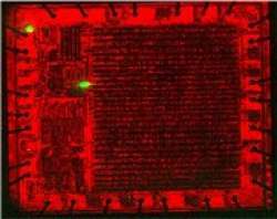
Emission microscopy (EMMI)
Emission microscopy (EMMI) is an efficient optical analysis technique used to detect and localize certain integrated circuit (IC) failures. Emission microscopy is non-invasive and can be performed from either the front or back of devices. Many device defects induce faint light emission in the visible and near infrared (IR) spectrum.
Emission microscopy uses a sensitive camera to view and capture these optical emissions, allowing device analysts to detect and localize certain IC defects. Since emissions can be detected from the back side, MuAnalysis uses an IR laser to create an overlay image of circuitry through the die. This allows failures to be related directly to circuit features, speeding failure resolution. A typical EMMI photo consists of an overlay of two images: the circuitry and the emission spots. Each is arbitrarily colorized a different way for clarity.
Emission microscopy is a powerful early-stage failure analysis technique. It localizes failures non-invasively and requires little in the way of sample preparation. Flip-chip devices, difficult to study by other means, are easily studied through the die without requiring decapsulation and often without thinning.
Typical applications
Detection of:
Overcurrent or ESD-induced damage
Hot electron susceptibility
Leakage current
Defective junctions
Forward-biased bipolar transistors
Latch-up
Floating gates
Flip-chip failure analysis

Front side emission

Back side emission
