
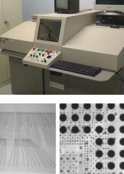
X-Ray Imaging
Real-time x-ray imaging is done in transmission and the image can be captured using film or an x-ray imaging system. The sample may be rotated to allow various perspectives, within the limitations of the sample size and geometry.
X-ray imaging is a quick, non-destructive analysis technique to look at solder joint quality and the large scale structure of devices.
Equipment
100kV x-ray imaging system upgraded to 1024x1024 pixel CMOS sensor
X-ray on film for military applications
3D x-ray available by special request
If defects are detected, recommendations are made for further tests or analyses.
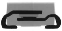
Bond wires in stacked Si chipsBalls and bumps of fcBGA
Semiconductor Diode
Typical applications
Failure analysis
Reverse engineering
Reliability analysis
Forensic analysis
Detection of:
Defects and voids in BGA balls, QFNs
Wire bonding defects
Metallization burnout
Voids in through hole pins.
Evaluation of:
Die attach integrity
Solder bump quality
Failure analysis
Reverse engineering
Reliability analysis
Forensic analysis
Detection of:
Defects and voids in BGA balls, QFNs
Wire bonding defects
Metallization burnout
Voids in through hole pins.
Evaluation of:
Die attach integrity
Solder bump quality